 (click to close) |
||
(click to close) |
||
 (click to close) |
||
 (click to close) |
||
 (click to close) |
||
|
|
||||||||||||
Sigma Projection |
||||||||||||
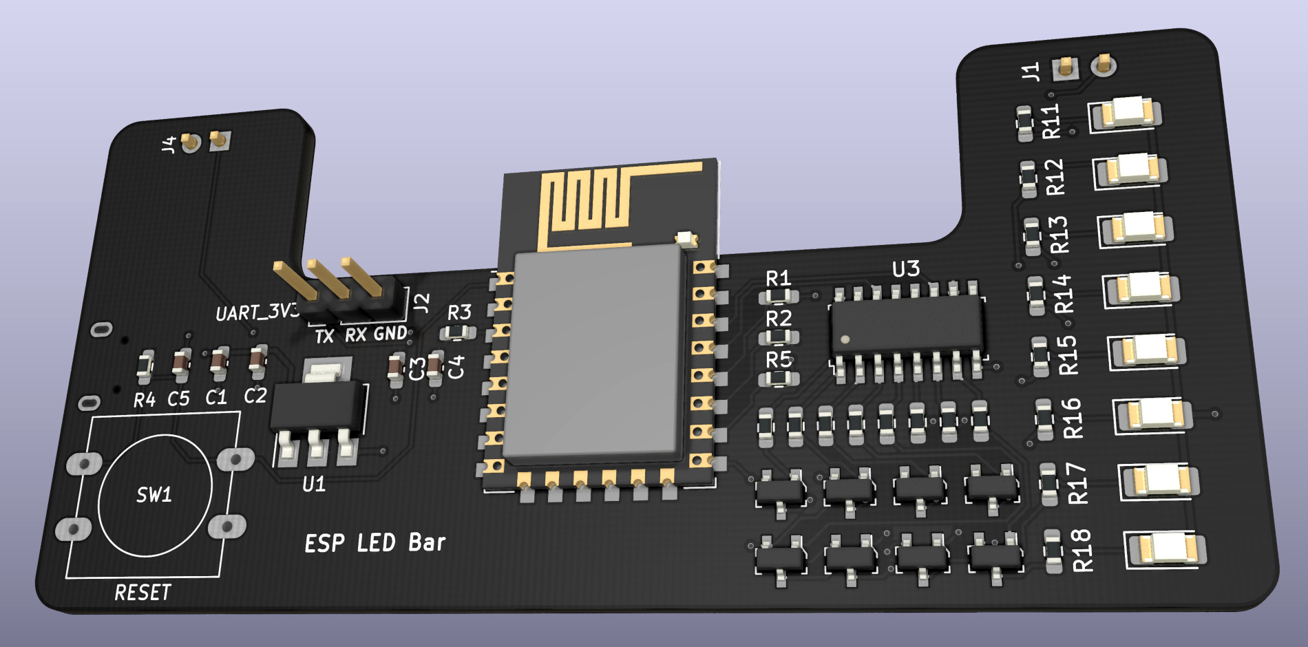
ESP-12E \ ESP-12F LED Bar PCBThis page represents overall design concepts of generic ESP8266 LED bar. Which is built based on ESP-12E \ ESP-12F module. This LED bar consists of 8 diodes which makes it usable in multiple applications to indicate various values. PCB can be used for values monitoring such as relative temperature, humidity, highway traffic congestion, etc. Source KiCad project and Gerber files are available on GitHub:
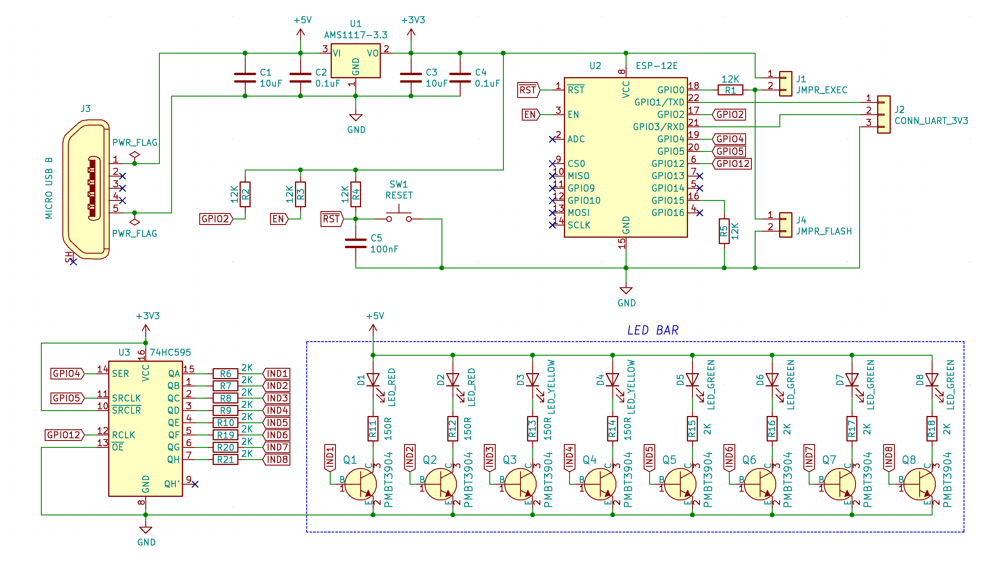
Gerber files can be downloaded from this site as well: [ ESP-12E(F) LED Bar PCB: Gerbers ] Overall LED Bar Design ConceptESP8266 module has quite limited amount of GPIO output pins which could be used to control set of LEDs. To overcome this problem we can use Shift Register 74HC595 chip which can play a role of serial to parallel converter. This way, we can allocate just 3 pins from ESP module to control any amount of LED - as 74HC595 Shift Registers can be cascaded into array using QH' pin. Under current design there is need to control just 8 LEDs, so one single 74HC595 register should be sufficient for these purposes. This is KiCad Schema design represending LED Bar PCB (click to enlarge):
The main purpose to drive LEDs on a separate 5V rail - to do not put extra load on AMS1117-3.3 module. Also green LEDs do have quite large voltage drop which can be more than 2V. In case of LEDs will be driven by 3.3V then slight difference in LEDs voltage drop can have increased current value deviation from expected value (hence deviation in brightness). This happens when the same value is used for all current limiting resistors. Driving LEDs by 5V rail will make this deviation negligible. This schema also has some room for optimization as amount of NPN transistors can be reduced from 8 to 3 which currently are used as a voltage level shift from 3.3V to 5V to drive LEDs. New PCBs revisions would include this change, but for now it can be kept for you to optimize as a practice exercise. Sample Application for TestingOnce PCB is ready and everything is soldered, it is a good practice to test its functionality. In case of our PCB - there is a need to make sure that 74HC595 shift register is working fine. Sample testing application has been created for these purposes, once testing application is uploaded it will try to ignite all LEDs one-by-one, sequentially. At this point it is possible to inspect LEDs behaviour manually, to make sure that all LED can be ignited and to make sure that 74HC595 shift register can ignite them in a sequence. PCB testing application is presented below: Sample Testing Application
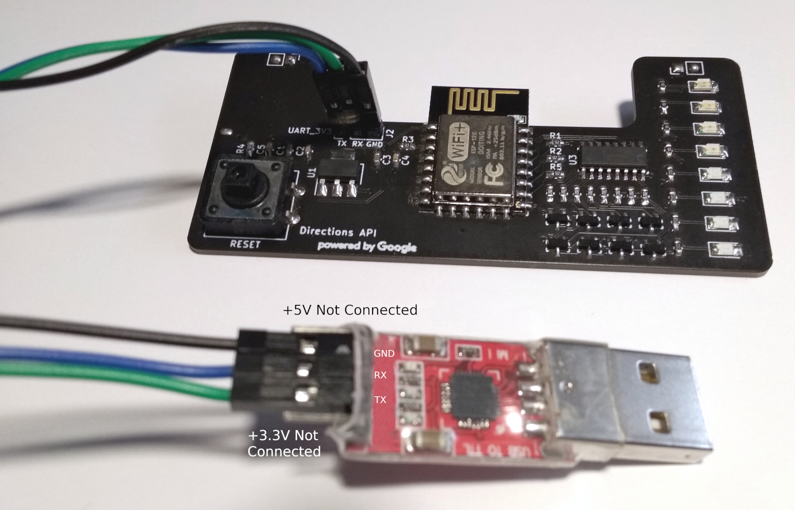
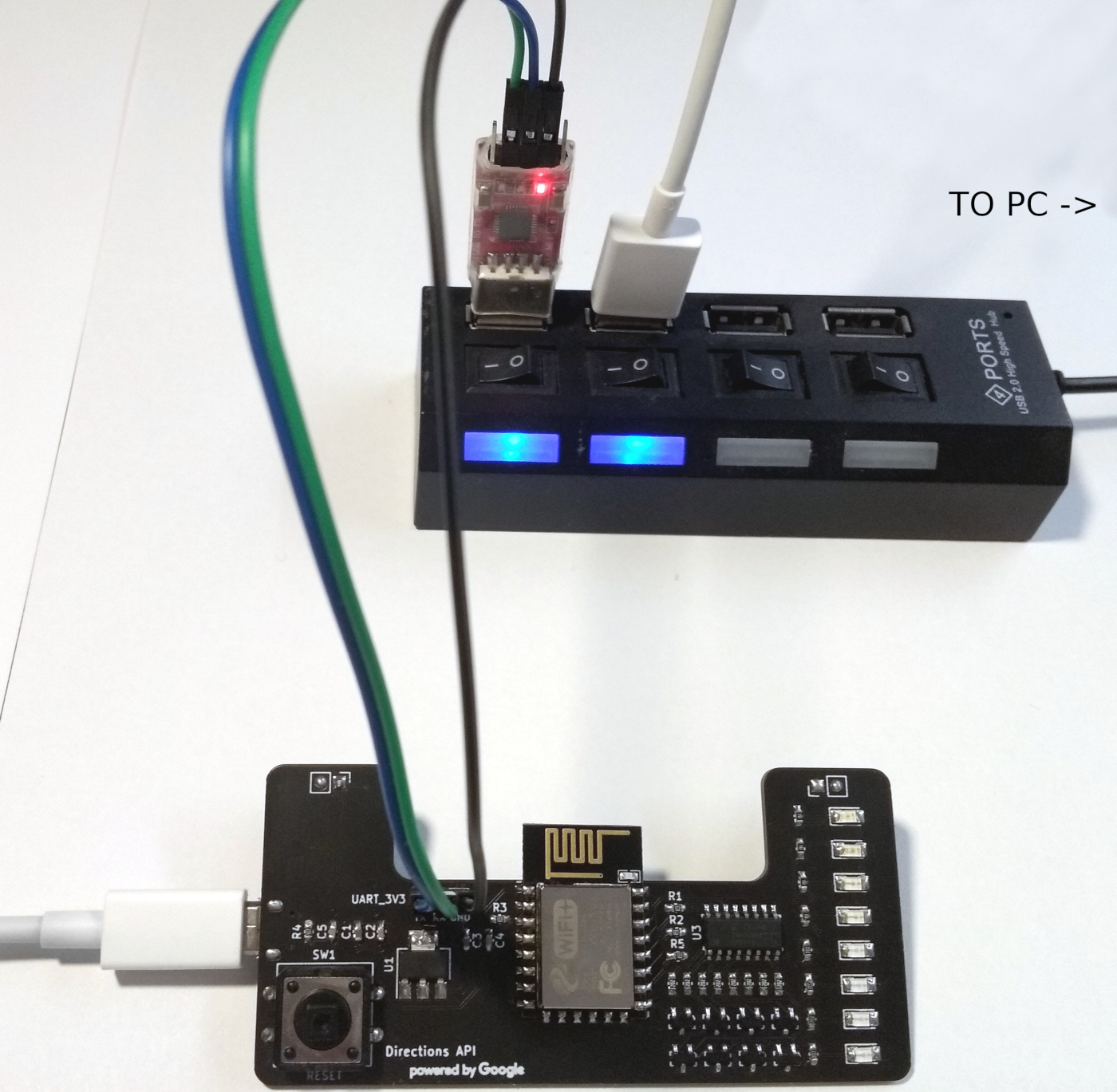
#include <osapi.h>
#include <user_interface.h>
#include <gpio.h>

#define LED_COUNT                               8

#define SYSTEM_PARTITION_RF_CAL_SZ              0x1000
#define SYSTEM_PARTITION_PHY_DATA_SZ            0x1000
#define SYSTEM_PARTITION_SYSTEM_PARAMETER_SZ    0x3000
#define SYSTEM_SPI_SIZE                         0x400000
#define SYSTEM_PARTITION_RF_CAL_ADDR            0x3FB000
#define SYSTEM_PARTITION_PHY_DATA_ADDR          0x3FC000
#define SYSTEM_PARTITION_SYSTEM_PARAMETER_ADDR  0x3FE000

// ESP pin connected to Shift Register 'SERIAL DATA' line
static const uint16 GPIO_PIN_SER_DATA   = 4;
// ESP pin connected to Shift Register 'SERIAL CLOCK' line
static const uint16 GPIO_PIN_SER_CLOCK  = 5;
// ESP pin connected to Shift Register 'READ LATCH' line
static const uint16 GPIO_PIN_READ_LATCH = 12;
// ESP internal LED pin number
static const uint16 GPIO_PIN_LED        = 2;

static const uint32 TIMER_IDX_RESET     = 1000000000;

// Delay in microseconds between Shift Register clock signals
static const uint16 DELAY_SHIFT_REG     = 50;

// This timer is used to update LED bar status
static os_timer_t start_timer;
// Initial timer tick value
static uint32 tick_index = 0L;

static const partition_item_t part_table[] =
{
    { SYSTEM_PARTITION_RF_CAL,              SYSTEM_PARTITION_RF_CAL_ADDR,           SYSTEM_PARTITION_RF_CAL_SZ              },
    { SYSTEM_PARTITION_PHY_DATA,            SYSTEM_PARTITION_PHY_DATA_ADDR,         SYSTEM_PARTITION_PHY_DATA_SZ            },
    { SYSTEM_PARTITION_SYSTEM_PARAMETER,    SYSTEM_PARTITION_SYSTEM_PARAMETER_ADDR, SYSTEM_PARTITION_SYSTEM_PARAMETER_SZ    }
};

// ############################# LED BAR - DISPLAY LEVEL  #############################

static void show_level(uint16 level)
{
    uint16 i;
    for (i = 0; i < LED_COUNT; ++i)
    {
        GPIO_OUTPUT_SET(GPIO_PIN_SER_DATA, (i < level));
        os_delay_us(DELAY_SHIFT_REG);
        GPIO_OUTPUT_SET(GPIO_PIN_SER_CLOCK, 1);
        os_delay_us(DELAY_SHIFT_REG);
        GPIO_OUTPUT_SET(GPIO_PIN_SER_CLOCK, 0);
        os_delay_us(DELAY_SHIFT_REG);
    }
    GPIO_OUTPUT_SET(GPIO_PIN_READ_LATCH, 1);
    os_delay_us(DELAY_SHIFT_REG);
    GPIO_OUTPUT_SET(GPIO_PIN_READ_LATCH, 0);
    os_delay_us(DELAY_SHIFT_REG);
}

// ################ APPLICATION MAIN LOOP METHOD (TRIGGERED EACH SECOND) ################

void main_timer_handler(void* arg)
{
    show_level(tick_index % (LED_COUNT + 1));
    ++tick_index;
    if (tick_index >= TIMER_IDX_RESET)
    {
        tick_index = 0;
    }
}

// ####################### APPLICATION MAIN INIT METHODS ################################

void ICACHE_FLASH_ATTR user_pre_init(void)
{
    system_partition_table_regist(part_table, 3, SPI_FLASH_SIZE_MAP);
}

void on_user_init_completed(void)
{
    // Timer setup to trigger each second
    os_timer_setfn(&start_timer, (os_timer_func_t*)main_timer_handler, NULL);
    os_timer_arm(&start_timer, 1000, 1);
}

void ICACHE_FLASH_ATTR user_init(void)
{
    gpio_init();
    // ESP pin modes initialization
    PIN_FUNC_SELECT(PERIPHS_IO_MUX_GPIO2_U, FUNC_GPIO2);
    PIN_FUNC_SELECT(PERIPHS_IO_MUX_GPIO4_U, FUNC_GPIO4);
    PIN_FUNC_SELECT(PERIPHS_IO_MUX_GPIO5_U, FUNC_GPIO5);
    PIN_FUNC_SELECT(PERIPHS_IO_MUX_MTDI_U, FUNC_GPIO12);
    // ESP pin values initialization
    GPIO_OUTPUT_SET(GPIO_PIN_LED, 0);
    GPIO_OUTPUT_SET(GPIO_PIN_SER_DATA, 0);
    GPIO_OUTPUT_SET(GPIO_PIN_SER_CLOCK, 0);
    GPIO_OUTPUT_SET(GPIO_PIN_READ_LATCH, 0);
    system_init_done_cb(on_user_init_completed);
}
Flashing and Running ESP ApplicationIn order to flash application into ESP module there is a need to use UART line connecting to 3-pins connector. This is due to designed PCB does not have any usb-to-serial adapter onboard. This UART connector also can be used in case of any application logs serial output needs to be monitored. This way, before flashing ESP8266 module there is a need to conduct the following steps:
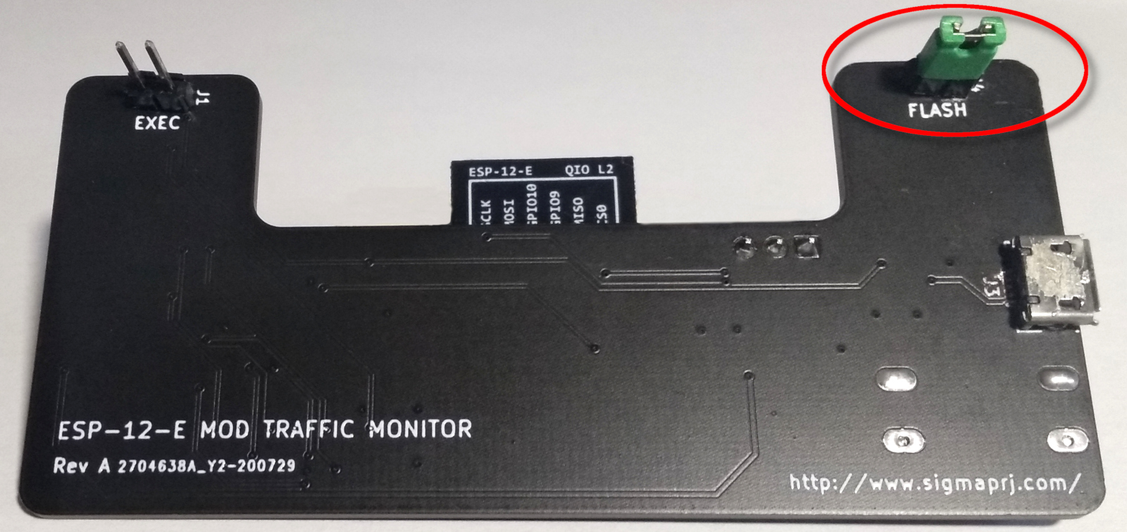
Once usb-to-serial adapter connection to PC is established, the sample application can be flashed. In order to write the program we can follow the steps which have been described in previous part about Custom ESP-12-E PCB Design. Further details on how ESP-12-E module can be flashed are available on YouTube video as well: ESP8266: How to design custom ESP-12E PCB. In order to pull-up GPIO0 pin (which is required to run the application) there is a need move jumper from FLASH to EXEC position. This way, after ESP chip reboot, the application will be executed on start-up. |